
Loading…
Layout Case Study
Buck Converter PCB Layout: 12 V to 3.3 V, Placement and Thermal
A 3.3 V, 3 A step-down converter laid out on two layers in 32.4 by 25.4 mm. The board carries the TI LMQ66430R5RXBR on a 0.41 mm FR-4 stack, holds the input capacitor 3.3 mm from the VIN and PGND pins, and uses the bottom layer as both ground plane and heatsink.
- Outline
- 25.4 × 32.4 mm
- Stackup
- 2-layer FR-4, 0.41 mm, 1 oz
- Input Capacitor
- 3.3 mm from VIN and PGND
- Thermal Path
- One 0.71 mm via into the plane
- Terminals
- 5 mm screw, opposite edges
- CAD Deliverable
- glTF 2.0 / STEP / Gerber X2
Interactive model
Inspect the delivered envelope
Orbit the board and look along the connector edge. The viewer loads the published glTF 2.0 binary, so the console renders exactly what a receiving CAD system imports: the board body, the connector body and the component envelope.
Stackup
Two Layers, One Plane
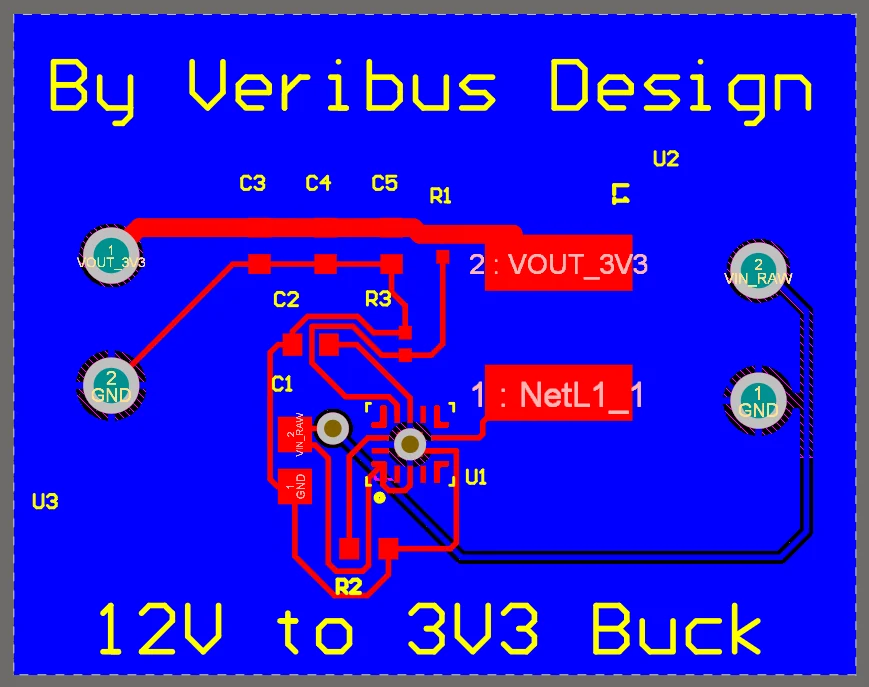
The board is 32.4 by 25.4 mm of 0.41 mm FR-4 with 1 oz copper on both sides. Every part is on the top layer, and so is every trace. The bottom layer is a ground plane and nothing else: it is the return path for the input loop, the reference for the feedback divider, and the heatsink for the regulator.
Two signal paths cross to the far side of the board, so the plane is split in two places, and both splits were routed away from the power stage. Switching current returns to C1 by the shortest route it can find, and a slot under that route sends it around the split instead. Under the converter, from input terminal to output terminal, the copper is continuous.
Two layers was enough for twelve parts and 3 A of output. A four-layer stack would have bought an inner plane this design did not need. What two layers costs is the return path: every via is a through via with a 0.71 mm hole in a 1.27 mm pad, so each layer change opens a hole in the plane underneath, and there are no stitching vias to give the return current a dedicated way back. The layout keeps layer changes off the sensitive nets instead.
Placement
The Input Loop And What Sits Where
C1, the 4.7 µF input capacitor, sits 3.3 mm from pins 3 and 6, on the same side as the regulator. That distance is the argument of a buck layout, because the loop through C1, the VIN pin, the two power FETs and PGND is the loop that radiates. At 3.3 mm the copper between the capacitor and the die behaves like copper rather than like an antenna.
The package does part of the work. VIN has two 22 nF capacitors in series to PGND inside the LMQ66430, so 11 nF sits at the die and handles the edge, and C1 is the bulk element behind it. That is what makes one 0805 sufficient instead of a bank of them. Everything on one side is also the cheaper assembly, and it leaves the bottom layer free for the plane.
C2, the 1 µF capacitor on the internal LDO output, is 4.2 mm from pin 10 on the same side. VCC is not a switching node, so the distance matters less than C1's, but the internal LDO feeds the control loop and the pin cannot be left without its capacitor. Nothing is routed under the RT resistor, which keeps the frequency-setting node away from the switching copper.
The two screw terminals sit on opposite edges, VIN on the right and VOUT on the left, with the wire entries facing outboard and the blocks overhanging the board edge. Input and output on the same edge would make the load current run back past the input loop; on opposite edges it leaves from where it was made.
Copper
Thermal Path And Copper
The exposed pad is the entire thermal path: one through via, a 0.71 mm hole in a 1.27 mm pad, tied into the bottom plane. That pad has one job, conduction, so the connection into the plane wants to be as direct as the via allows. Relief spokes exist to make hand soldering easier, and here they would add thermal resistance exactly where the heat has to leave. That plane is the heatsink.
The via is also the path solder takes during reflow. Paste printed on that pad has to fill a 0.71 mm hole, and the stencil aperture there decides whether the joint ends up voided. It is worth looking at that pad under magnification before trusting any temperature measured on the part.
Copper width follows current, not schematic symbols. The output rail runs about 1 mm wide from the inductor past C3 to C5 and on to the output terminal, carrying . The input current is set by the conversion ratio:
At 12 V in and 3 A out that is just under 1 A, a third of the output current, so the 12 V side is routed as narrow traces and the 3.3 V side is not.
Build
Rev A, And What It Has Not Shown Yet
The board is Rev A, fabricated and assembled by JLCPCB, and the design rule check closed without errors or warnings. It has not been characterised: there is no efficiency sweep, no switch-node capture and no thermal image for it.
The switch node and the case temperature are where that work starts: 1.1 A of ripple at 2.2 MHz makes the switch node the busiest copper on the board, and the single via under the pad is the only route from the die to the plane that cools it. On a second spin I would add a pair of ground test points and a ring of stitching vias around the power stage.
FAQ
Common questions
Twelve parts and 3 A of output do not need inner planes, and the bottom layer already gives the power stage a continuous reference. The cost is the return path: through vias put 0.71 mm holes in the plane and there are no stitching vias, so the layout avoids layer changes on the sensitive nets instead.
Related Tools and Services
Have the Numbers Checked Against the Board
Send the stackup, the interface list and the manufacturing package inputs. An engineer re-solves them against the real layout before the fixed fee is issued.