
Loading…
Layout Case Study
USB-to-UART PCB Layout: A 90 Ohm Pair On A Four-Layer Stack
A 25.4 mm square bridge that takes USB 2.0 full speed from a Type-C receptacle to a four-pin UART header. Four layers at 0.55 mm with 0.5 oz copper, a continuous Layer 2 ground plane under the pair and the bridge, and a 90 Ω differential pair set from the stackup rather than copied from a table.
- Outline
- 25.4 × 25.4 mm
- Stackup
- 4-layer FR-4, 0.55 mm, 0.5 oz
- Reference Plane
- Continuous Layer 2 ground
- Differential Pair
- 90 Ω target, 0.126 / 0.127 mm
- Revisions
- Rev B, two builds
- CAD Deliverable
- glTF 2.0 / STEP / Gerber X2
Interactive model
Inspect the delivered envelope
Orbit the board and look along the connector edge. The viewer loads the published glTF 2.0 binary, so the console renders exactly what a receiving CAD system imports: the board body, the connector body and the component envelope.
Stackup
Four Layers At 0.55 mm
The board is 25.4 mm square and 0.55 mm thick, four layers of FR-4 with 0.5 oz copper throughout. Layer 1 is signal and carries every part, Layer 2 is a continuous ground plane, Layer 3 takes what has to escape the connector fanout, and Layer 4 is spare, there mainly to keep the stack symmetric.
The differential pair is 0.126 mm wide with a 0.127 mm gap. Both numbers came out of Altium's impedance profile for this stack and were then checked in a calculator. The pair only reaches 90 Ω because the plane is close, so a thin stack earns its place here. The boards were ordered with impedance control, and the 90 Ω figure is a design target rather than a measurement, because no TDR was run.
The rest of the routing is 0.25 mm, comfortably inside the 0.1 mm minimum JLCPCB offers on a four-layer board. The pair geometry came from the impedance profile rather than from a hand-written rule, and the Altium defaults covered everything else.
Placement
Floorplan: Connector, TVS, Bridge, Header
The Type-C receptacle is on the left edge, the four-pin UART header is on the right, and the CP2102N sits between them. The TVS array is above and between the connector and the bridge, which is the only position that puts it in the transient's path: current arrives at the connector, meets the clamp before it reaches the silicon, and then continues to the bridge. A TVS placed after the bridge protects the bridge from nothing.
Everything is on the top side, so the board goes through one reflow and the bottom layer stays free for the plane.
The bridge's exposed pad carries a single through via in the centre, enough for a part dissipating a fraction of a watt, and it avoids the via row a QFN pad usually gets, each of which would be a 1.27 mm hole in the plane directly under the device.
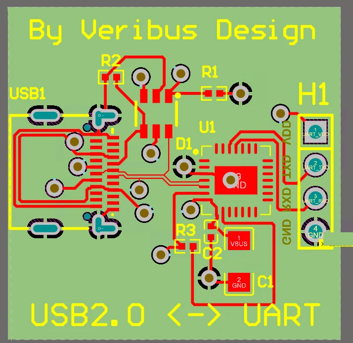
Layer 2
The Pair And Its Return Path
Layer 2 has no splits under the pair and none under the bridge. That is the rule that matters for a differential pair: the return current runs directly beneath each trace, and anything that interrupts the plane both radiates and changes the impedance mid-run.
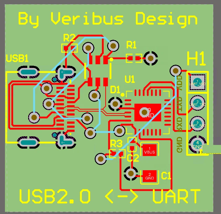
The plane is not perfect: through-hole connector pins cut into it at the Type-C footprint and at the header, and every signal via is a through via with a 0.71 mm hole in a 1.27 mm pad, so each one opens a clearance circle in the plane underneath. There are no stitching vias to put that copper back. The pair therefore stays on Layer 1 from connector to bridge, and the escapes that would have forced a transition were pushed down to Layer 3 instead.
Layer 3 is where the fanout goes. The Type-C footprint puts two rows of pads in a small area, and the bridge's pins have to reach the header on the far edge, so the inner layer carries those runs while the pair keeps its reference plane intact below it.
Bring-Up
Testing
Rev B enumerated on a host as a CP2102N bridge, and a loopback across the header ran at 115,200 baud with the bytes coming back as expected. That is the whole test record: the host log is a real capture, trimmed to the lines showing the device attach and the driver bind.
It is a functional check, not a characterisation: nothing was measured on the pair, no eye or TDR was taken, and the loopback was watched rather than error-counted. The layout claims here rest on the stackup and the geometry, not on a waveform.
What Changed
Rev B, And Why It Exists
Rev A had the TVS array wired wrong: VBUS landed on one of the IO protection lines, and D- landed on the array's positive rail. The datasheet numbers the pins instead of naming them, and the symbol arrived with no pin names either, so the block diagram was the only place the pin functions were written down. Reading it turned a five-pin part with one obvious ground into five pins doing five different jobs.
Both revisions were fabricated and assembled by JLCPCB. The episode is a reminder that a protection array is a wiring constraint before it is a layout one: the clamp only protects if the pin facing the connector is the pin the clamp sits on.
FAQ
Common questions
Layer 2 is the reason. A continuous plane under the pair and the bridge keeps the impedance stable and the return current where it belongs, and the Type-C fanout needs an inner layer to escape without cutting that plane. The fourth layer keeps the stack symmetric.
Related Tools and Services
Have the Numbers Checked Against the Board
Send the stackup, the interface list and the manufacturing package inputs. An engineer re-solves them against the real layout before the fixed fee is issued.